Logic Gates#
All gates can be derived from the NAND GATE.
What is NAND GATE?
A NAND GATE is a switch that follows the following truth table.
NAND GATE#
A |
B |
\(\bar{AB}\) |
|---|---|---|
0 |
0 |
1 |
0 |
1 |
1 |
1 |
0 |
1 |
1 |
1 |
0 |
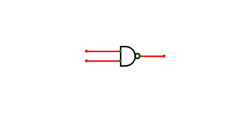
This is a circuit diagram of the NAND GATE.
Next up, is the NOT GATE. The gate should invert signals sent to it. Which gives us a hint of how to design the ciruit.
NOT GATE#
A |
\(\bar{A}\) |
|---|---|
0 |
1 |
1 |
0 |
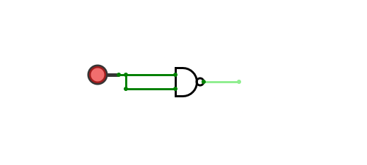
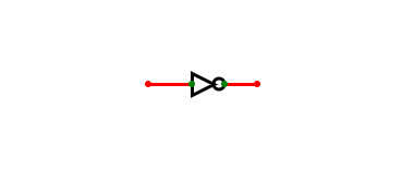
This is a circuit diagram of the NOT GATE. The inputs into the NAND GATE come from both a single input. It is then drawn as a triangle with a circle at the tip.
OR GATE#
A |
B |
A+B |
|---|---|---|
0 |
0 |
0 |
0 |
1 |
1 |
1 |
0 |
1 |
1 |
1 |
1 |
The OR GATE can be built using 3 NAND GATES. Both inputs are mapped into a NAND GATE then the output of both gate are then inverted.
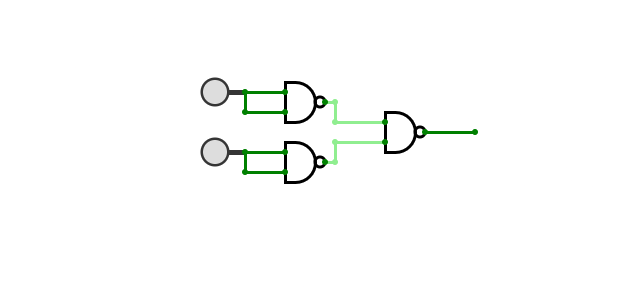
This is a circuit diagram of the OR GATE made from NAND GATES.
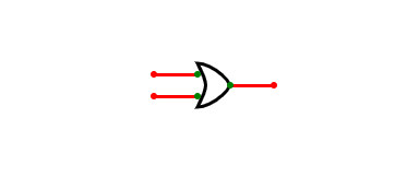
This is a circuit diagram symbol of the OR GATE.